Graphene Potential in Next-Generation Electronics

Explore the transformative potential of graphene in next-generation electronics as we delve into its remarkable properties, challenges in commercialization, future applications, and research directions. Discover how graphene, a two-dimensional carbon allotrope, is revolutionizing the electronics industry with its exceptional conductivity, flexibility, and transparency. Dive into the article to uncover the latest advancements, potential applications, and strategies for overcoming challenges in commercializing this groundbreaking material.
What is Graphene?
Graphene is a remarkable material consisting of a single layer of carbon atoms arranged in a two-dimensional honeycomb lattice. It is often hailed as a wonder material due to its extraordinary properties, which include exceptional strength, electrical conductivity, thermal conductivity, and flexibility. Graphene’s unique structure and composition give rise to its remarkable characteristics, making it a highly sought-after material for various applications in electronics, energy storage, biomedical engineering, and more.
Graphene Discovery and Early Studies
The discovery of graphene can be attributed to the pioneering work of Professor Andre Geim and Professor Kostya Novoselov at the University of Manchester. In 2004, the two scientists successfully isolated graphene by mechanically exfoliating graphite using adhesive tape, a technique known as the “Scotch tape method.” This breakthrough began intensive research into graphene’s properties and potential applications.
Early studies on graphene focused on characterizing its structural and electronic properties. Researchers used techniques such as transmission electron microscopy (TEM), scanning tunneling microscopy (STM), and Raman spectroscopy to investigate graphene’s atomic structure, electronic band structure, and phonon properties. These studies revealed graphene’s unique properties, including its remarkable strength, high electron mobility, and optical transparency.
Graphene Structure and Composition
Graphene’s structure consists of a hexagonal lattice of carbon atoms arranged in a single layer, with each carbon atom forming three covalent bonds with neighboring atoms. The resulting lattice resembles a honeycomb pattern, giving graphene its distinctive two-dimensional structure. Graphene can be visualized as a single layer of graphite, commonly found in pencil lead.
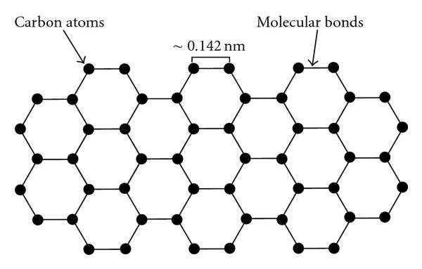
The carbon-carbon bonds in graphene are exceptionally strong, providing the material with remarkable mechanical properties. Graphene is one of the strongest materials known, with a tensile strength exceeding that of steel by several orders of magnitude. Additionally, graphene exhibits high electrical conductivity due to its unique electronic band structure, where electrons behave as massless Dirac fermions.
Graphene’s composition consists solely of carbon atoms, arranged in a flat, single-layer structure. Each carbon atom in graphene forms sp² hybridized bonds with three neighboring atoms, resulting in a planar lattice with strong covalent bonds. The absence of impurities or defects in its pristine form contributes to graphene’s exceptional mechanical, electrical, and thermal properties.
Properties of Graphene
Graphene possesses many exceptional properties, making it a highly desirable material for various applications. Some of the key properties of graphene include:
- Exceptional Strength: Graphene is one of the strongest materials known to mankind, with a tensile strength exceeding that of steel by several orders of magnitude. This exceptional strength arises from the strong covalent bonds between carbon atoms in its two-dimensional honeycomb lattice structure.
- High Electrical Conductivity: Graphene exhibits remarkable electrical conductivity, with electrons able to travel through its structure at extremely high speeds. This property makes graphene an excellent conductor of electricity, surpassing even copper and other traditional conductive materials.
- High Thermal Conductivity: Graphene also demonstrates high thermal conductivity. It can efficiently dissipate heat, making it suitable for effective thermal management applications.
- Optical Transparency: Despite being just one atom thick, graphene is optically transparent, allowing light to pass through with minimal absorption. This property is ideal for applications requiring transparent conductive coatings, such as touchscreens and solar panels.
- Flexibility and Mechanical Resilience: Despite its exceptional strength, graphene is incredibly flexible and can be bent, stretched, or twisted without losing its structural integrity. This flexibility and mechanical resilience make graphene an excellent candidate for flexible electronics and wearable devices.
- Large Surface Area: Graphene has an extensive surface area due to its two-dimensional structure, offering ample space for chemical interactions. This property makes graphene well-suited for gas sensing, catalysis, and energy storage devices like supercapacitors.
- Impermeability: Graphene is impermeable to gases and liquids, even at the atomic scale. This property makes it useful for applications requiring barrier properties, such as protective coatings and membranes for gas separation.
Graphene’s Role in Next-Generation Electronics
Graphene’s exceptional properties position it at the forefront of next-generation electronics, offering numerous advantages over traditional materials. Some of the key roles of graphene in advancing electronics include:
- High-Speed Electronics: Graphene’s high electrical conductivity and electron mobility make it ideal for high-speed electronic devices, such as transistors and interconnects, enabling faster data processing and transmission.
- Flexible Electronics: Graphene’s flexibility and mechanical resilience enable the development of flexible electronic devices that can conform to curved surfaces or be integrated into wearable technology, opening up new possibilities for personalized electronics and healthcare monitoring.
- Transparent Conductive Films: Graphene’s optical transparency and high electrical conductivity make it an excellent candidate for transparent conductive films used in touchscreens, displays, and solar cells, offering improved performance and durability compared to traditional materials like indium tin oxide (ITO).
- Energy Storage and Conversion: Graphene’s large surface area, high electrical conductivity, and electrochemical stability make it an ideal material for energy storage and conversion devices, such as supercapacitors, batteries, and fuel cells, enabling higher energy densities and faster charging rates.
- Sensors and Detectors: Graphene’s high sensitivity to environmental changes, combined with its large surface area and electrical conductivity, make it well-suited for sensors and detectors used in various applications, including environmental monitoring, healthcare diagnostics, and aerospace.
- Thermal Management: Graphene’s high thermal conductivity and mechanical flexibility make it effective for thermal management applications in electronics, such as heat sinks, thermal interface materials, and flexible thermal substrates, improving the performance and reliability of electronic devices.

Graphene as a Semiconductor
In addition to its conductor role, graphene exhibits semiconductor properties, making it suitable for electronic devices that require switching capabilities. Some key points regarding graphene’s role as a semiconductor include:
- Tunable Bandgap: Graphene’s electronic band structure can be modified to introduce a bandgap, enabling it to function as a semiconductor. This tunable bandgap allows for the design of graphene-based electronic devices, such as transistors and diodes, with enhanced switching capabilities and reduced leakage currents.
- Ambipolar Transport: Graphene exhibits ambipolar transport, meaning it can carry both positive (holes) and negative (electrons) charge carriers simultaneously. This property enables the design of graphene-based transistors capable of operating in both n-type and p-type modes, offering greater flexibility in device design and functionality.
- High Carrier Mobility: Graphene’s high carrier mobility, resulting from its two-dimensional structure and lack of impurities, allows for efficient charge transport in semiconductor devices. This high carrier mobility enables faster switching speeds and lower power consumption in graphene-based transistors, improving the overall performance of electronic circuits.
- Edge States and Quantum Confinement: Graphene’s edges exhibit unique electronic properties due to unsaturated carbon atoms. These edge states can be manipulated to introduce quantum confinement effects, enabling the design of graphene-based quantum devices with novel electronic and optical properties.
- Heterostructures and van der Waals Heterojunctions: Graphene can be combined with other two-dimensional materials, such as transition metal dichalcogenides (TMDs) and hexagonal boron nitride (h-BN), to create heterostructures and van der Waals heterojunctions with tailored electronic properties. These heterostructures hold promise for developing advanced semiconductor devices, including tunneling transistors, photodetectors, and optoelectronic devices.
Graphene-Based Transistors
Transistors are fundamental building blocks of electronic circuits, which amplify or switch signals in various electronic devices. Graphene-based transistors offer several advantages over traditional silicon transistors, including higher electron mobility, faster switching speeds, and lower power consumption. Some of the key features and advancements in graphene-based transistors include:
- High Electron Mobility: Graphene exhibits exceptional electron mobility, with electron velocities exceeding 10^5 m/s at room temperature. This high electron mobility enables graphene-based transistors to achieve faster charge transport and switching speeds than silicon transistors.
- Ballistic Transport: In graphene-based transistors with short channel lengths, electrons can travel ballistically without scattering, leading to ultrafast electron transport and minimal delay. This ballistic transport behavior allows for the fabrication of high-speed graphene transistors with superior performance.
- Ambipolar Transport: Graphene-based transistors exhibit ambipolar transport, where electrons and holes contribute to current conduction. This ambipolar behavior is advantageous for certain transistor configurations and device applications, enabling the development of versatile graphene-based electronic devices.
- Tunable Bandgap: Graphene’s electronic band structure can be engineered to introduce a bandgap, allowing for the fabrication of graphene-based field-effect transistors (FETs) with improved switching characteristics. By controlling the doping level, strain, or heterostructure configuration, the bandgap of graphene-based transistors can be tailored for specific device applications.
- Flexible and Transparent Transistors: Graphene’s flexibility and transparency make it an ideal material for flexible and transparent transistors, which can be integrated into bendable, stretchable, and see-through electronic devices. Graphene-based transparent transistors offer new opportunities for developing innovative display technologies, wearable electronics, and transparent sensors.
- Scalability and Integration: Graphene-based transistors can be fabricated using scalable manufacturing techniques, such as chemical vapor deposition (CVD) and transfer printing, enabling large-scale production and integration into existing semiconductor manufacturing processes. Graphene’s compatibility with complementary metal-oxide-semiconductor (CMOS) technology further facilitates its integration into mainstream electronics.
- Low Power Consumption: Graphene-based transistors exhibit low power consumption due to graphene’s high electron mobility and ballistic transport behavior. This low power consumption is particularly advantageous for high-speed and energy-efficient electronic devices, such as high-frequency amplifiers, radio-frequency (RF) switches, and low-power sensors.
Graphene-Based Sensors
Graphene-based sensors are electronic devices that utilize graphene’s unique properties to detect and measure various physical, chemical, biological, and environmental stimuli. Graphene’s high surface-to-volume ratio, exceptional electrical conductivity, and sensitivity to external perturbations make it an ideal material for sensing applications. Some of the key features and advancements in graphene-based sensors include:
- High Sensitivity: Graphene-based sensors exhibit high sensitivity to small environmental changes, enabling detecting and measuring minute quantities of analytes or stimuli. Graphene’s high surface-to-volume ratio allows efficient interaction with target molecules or particles, enhancing sensor sensitivity.
- Fast Response Times: Graphene-based sensors offer fast response times, with rapid detection and measurement of target analytes or stimuli. Graphene’s high electrical conductivity and low mass facilitate fast charge transfer and signal transduction, resulting in quick sensor response times.
- Low Detection Limits: Graphene-based sensors can achieve low detection limits for target analytes or stimuli, owing to their high sensitivity and signal-to-noise ratio. Graphene’s exceptional electrical conductivity allows for detecting weak electrical signals generated by the interaction between graphene and target molecules or particles.
- Wide Dynamic Range: Graphene-based sensors exhibit a wide dynamic range, capable of detecting a broad range of analyte concentrations or stimuli intensities. Graphene’s tunable electronic properties and controllable surface chemistry optimize sensor performance across different concentration ranges.
- Selective Sensing: Graphene-based sensors can be functionalized or modified to achieve selective sensing of specific analytes or stimuli. By incorporating molecular recognition elements or surface modifiers onto graphene’s surface, sensors can selectively bind to target molecules or particles, enabling precise detection and measurement.
- Multiplexed Sensing: Graphene-based sensors can be integrated into multiplexed sensing platforms, allowing for simultaneous detection and measurement of multiple analytes or stimuli. Graphene’s compatibility with microfabrication techniques and electronic readout systems enables the development of compact and portable sensor arrays for diverse applications.
- Flexible and Wearable Sensors: Graphene’s flexibility and mechanical strength make it suitable for flexible and wearable sensor applications. Graphene-based sensors can be integrated into clothing, textiles, or wearable accessories, enabling real-time monitoring of physiological parameters, environmental conditions, or hazardous substances.
- Miniaturized Sensors: Graphene-based sensors can be miniaturized to nanoscale dimensions, offering high spatial resolution and sensitivity for localized sensing applications. Graphene nanosensors can detect and measure analytes or stimuli at the nanometer scale, facilitating advanced imaging, diagnostics, and biomedical applications.
Overcoming Challenges: Commercialization and Scalability
Despite the promising properties of graphene, its widespread commercialization and scalability face several challenges that need to be addressed. Overcoming these challenges is crucial for realizing the full potential of graphene in various industries, including electronics.
- Material Quality and Consistency: Ensuring consistent quality and properties of graphene across large-scale production remains a challenge. Variations in synthesis methods and impurities can affect the performance of graphene-based devices.
- Compatibility with Existing Technologies: Integrating graphene into existing manufacturing processes and device architectures without major modifications presents challenges. Adapting production lines and materials to incorporate graphene seamlessly requires research and development.
- Synthesis Methods: Current methods for large-scale graphene production, such as chemical vapor deposition (CVD) and liquid phase exfoliation (LPE), need refinement to achieve higher yields, lower costs, and better quality control.
- Scaling Up Production: Transitioning from lab-scale synthesis to industrial-scale production poses challenges in maintaining material quality, consistency, and cost-effectiveness. Scalable production techniques are essential to meet the growing demand for graphene-based materials.
- Compatibility with Substrates: Graphene’s integration with different substrates and materials used in electronic devices requires optimization to ensure compatibility, adhesion, and performance.
- Functionalization: Surface functionalization of graphene is essential for enhancing its compatibility with other materials and improving specific properties for targeted applications. Developing effective functionalization methods is crucial for broadening graphene’s utility in electronics.
- Material Cost: Despite advancements, graphene production costs remain relatively high compared to traditional materials used in electronics. Innovations in production techniques and economies of scale are needed to reduce production costs and improve cost-effectiveness.
- Manufacturing Processes: Optimizing manufacturing processes to minimize waste, energy consumption, and labor costs is essential for producing graphene-based electronic devices cost-effectively.
Conclusion
Graphene’s remarkable properties, including exceptional electrical conductivity, mechanical strength, flexibility, transparency, and biocompatibility, position it as a transformative material with diverse applications across various industries. From electronics and energy storage to biomedical devices and materials science, graphene offers unprecedented opportunities for innovation and advancement. As research progresses and technological advancements continue, the potential applications of graphene are expected to expand, leading to groundbreaking developments and transformative changes in how we harness and utilize materials for future technologies. By addressing challenges in synthesis, integration, scalability, and commercialization, graphene promises to enable a wide range of disruptive technologies that will shape the future of society and industry.


0 Comments